
here’s some background information and speculation, as someone not involved in the industy.
the silicon wafers used for making chips are big single crystals, which are made by the Czochralski method
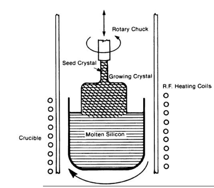 the crucible is also made of silica and needs to be very perfect, so that no crystals are seeded from the walls, so it makes sense to me that the crucible needs to be at least the purity of the desired silicon wafers - which is at least 99.9999% pure and for research-grade samples 99.99999999% pure. I suspect that the leading-edge nodes requires the high-end of this scale. Its economical to start with the highest purity material that you can, which according to Conway’s Material World comes from spruce pine, but its possible to use a lower grade starting material.


MEMS are also made of silicon.
quartz oscillators were basically the first MEMS.(i wrote that but actually its not true lol. something else cool is saw filters which kind of build on the concept of quartz oscillators btw) cool fact: the reason helium kills MEMS is because the atoms are so small that they can diffuse their way through the wall of the device, filling it up with helium and the air resistance then stops it from working!